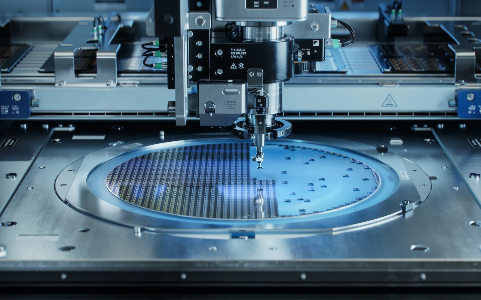
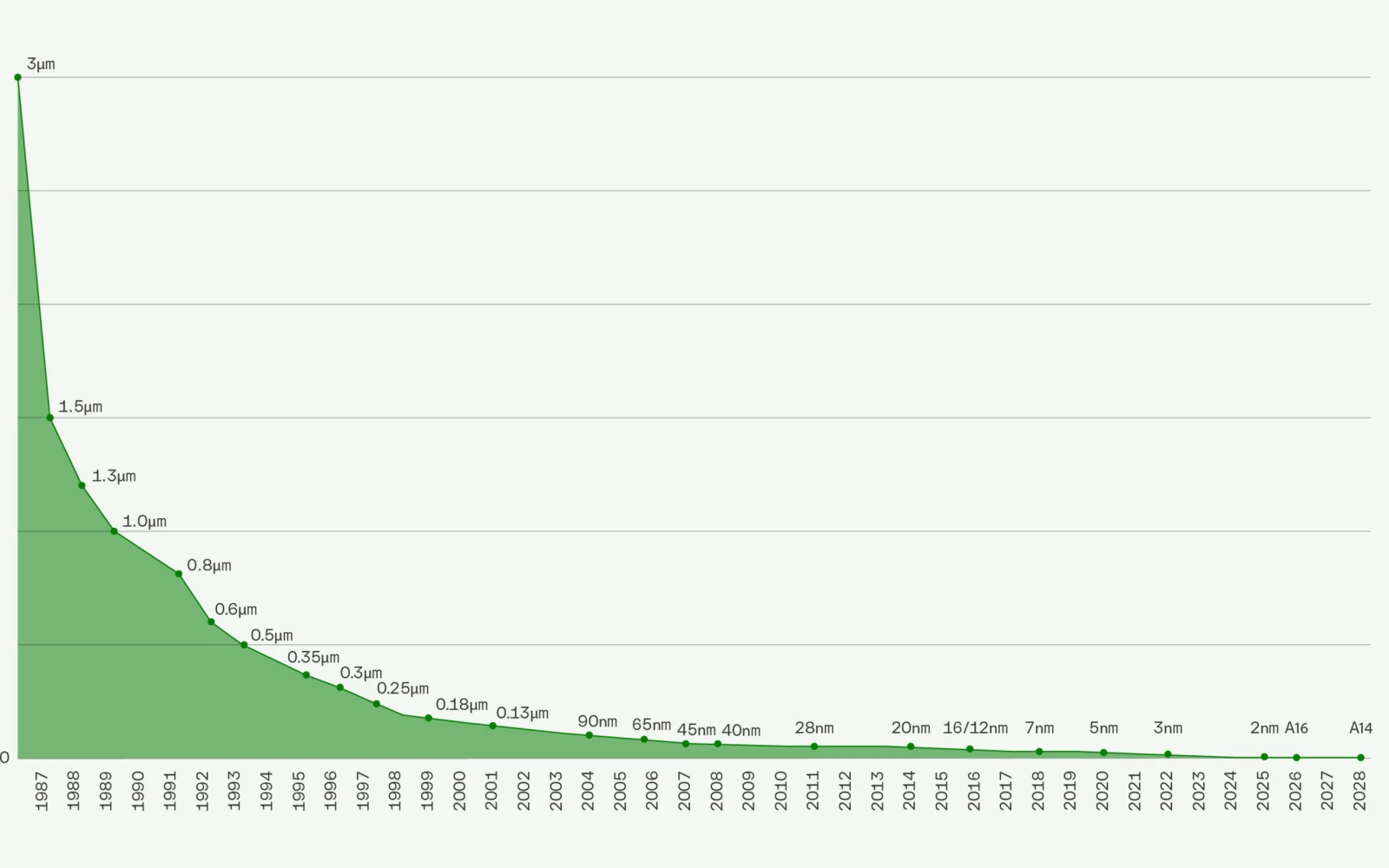
Manufacturing the CPUs and GPUs that power every mobile device or data center starts with the optical lithography machines companies use to build their chips. This equipment is among the most intricate and expensive machinery ever made. Transitioning from one generation of lithographic techniques to the next, to achieve greater feature density and extend Moore’s Law-style device scaling, is always an engineering tour de force.
Just reaching the current plateau — using extreme ultraviolet or EUV wavelengths to etch features at the 7‑nanometer scale and below — demanded sustained research over roughly two decades and many billions of dollars of cumulative R&D investment before production-ready tools emerged. Today’s commercial EUV lithography systems are manufactured by only one company, ASML, with optics from Carl Zeiss and lasers from Trumpf, and they can cost $200 million to $400 million each. The whole point of these machines is to create smaller and smaller features on silicon substrates. (Smaller transistors mean more of them can be crammed onto each chip; since the electrons travel shorter distances they’re more efficient as well.)
In traditional lithography, the only way to make features smaller is to use either shorter wavelengths of light or brighter light, or both. This light shines through and/or reflects off a patterned, stencil-like photomask, exposing a photoresist, which allows the patterned regions to be selectively removed so that the pattern can be etched into the underlying silicon. But as the EUV approach pushes toward smaller feature sizes (into the lowsingle-digit nanometer regime), it’s hitting fundamental limits. Defects in photoresist chemistry and noise from individual photons constrain the precision and resolution of lines and other features.
One feasible way to keep going smaller is to switch to a different lithographic regime altogether. What if the photomask were no longer a passive stencil? Future nanoscale photomask architecture could sculpt and reshape the electromagnetic field from visible light (not EUV), concentrating energy into localized pockets on the photoresist far smaller than the light’s wavelength. If the mask were to become an active optical device— not just a shadow- or reflection-caster — it might be possible to achieve features as small as 2 – 4 nm, without the high-energy lasers or vacuum conditions required in EUV. “Foundational tech for heavy compute has a number of layers, starting all the way down with the semiconductor layer,” says DCVC General Partner Ali Tamaseb. “New mask methods would enable better and finer lithography.”
The next way to create chips capable of more operations per second, and at higher energy efficiency, is to think multi-dimensionally. “We either need to go smaller, or we need to build up, like a city with multiple levels,” Tamaseb explains.
As an example, chip designers are exploring stacking integrated circuits and building blocks called chiplets to create dense multi-layer designs. These can shorten interconnect distances and allow logic, memory, and other components to be interspersed. The overall idea is to extract more performance and energy efficiency by rethinking how chips are physically organized, not just how finely they’re etched. Advanced chipmakers like TSMC, Intel, and Samsung are active here, as are newer companies such as Ayar Labs, which specializes in fast optical interconnects for chiplets.
The infrastructure layer of the AI stack is becoming interesting and investable.”
Zachary Bogue
Co-Founder and Managing Partner, DCVC
When processor speed and efficiency are paramount, there’s also room to bet on more disruptive approaches. One of them is to change the way computers handle the basic math behind machine learning. And it turns out that running that math on analog rather than digital hardware is dramatically more energy-efficient, as our portfolio company Mythic is demonstrating.
Modern ML hardware performs one dominant class of calculations over and over: matrix multiplication and accumulation, where input activations are multiplied by an array of neural network weights. In a digital AI chip that means fetching the weights from memory, fetching the activations as well, then multiplying and adding up the answers in logic and reading out the results. The problem is that in energy terms, all this fetching of data is orders of magnitude more expensive than the actual arithmetic. “We need better ways to reduce the cost of data movement,” says Tamaseb. “Mythic has solved it in one way by bringing together compute and memory in the same place.”
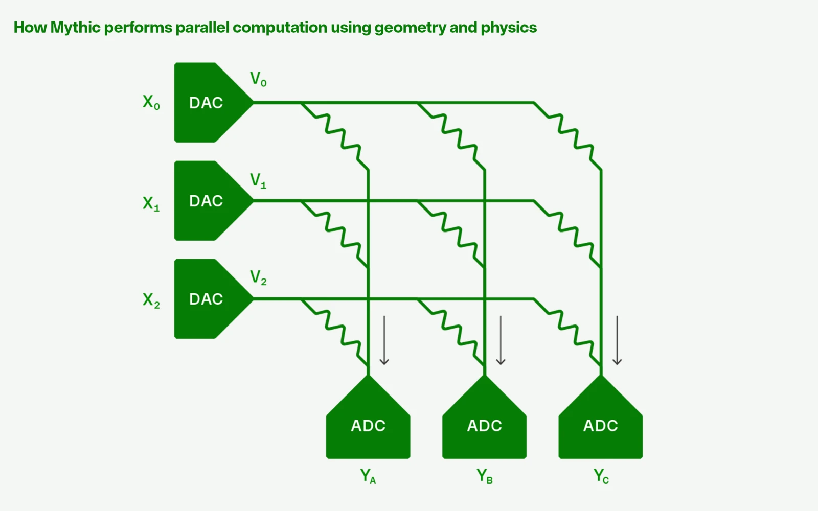
Mythic’s analog chips are, in fact, memory arrays, wired up so that circuit physics performs the math. A Mythic chip is an array of non-volatile analog flash memory elements connected in rows and columns and operated as tunable resistors. Neural network weights are represented in the array by setting the flash cells at different levels of conductance. Input activations are applied along the rows as voltages, and at each element, the voltage drives a current whose magnitude is set by the conductance — the physical equivalent of a multiplication. These currents flow along a shared column, where readout circuitry captures the final sums. Far less data moves at all; the array itself carries out a massively parallel computation by virtue of geometry, Ohm’s Law, and Kirchhoff’s current law.
Mythic’s M1076 compute-in-memory chip can deliver AI throughput comparable to an edge GPU for 1/10th of the power, and the company says its next-generation analog processing units are targeted to be up to 100 times more energy-efficient than conventional digital GPUs. That means tasks like AI inference that used to be confined to data centers can increasingly happen at the network’s edges, where computing meets the environment— think drones, smart city and smart home devices, and especially robots. “We’re going to see robotics actually take off because edge compute is becoming a thing,” Tamaseb predicts. “It used to be that you couldn’t run all of this compute on these robots — you had to send it to the cloud, and you had latency problems. Now we are able to actually use top models, big AI models, on the edge, running directly on these robots with low latency. That’s going to be a big unlock.”
Another potentially transformative edge computing application: brain-computer interfaces. Here we’re watching companies such as Infera Neuro, a spinoff from École Polytechnique Fédérale de Lausanne (EPFL) in Switzerland. They’re developing tiny, low-power implantable AI chips that could read brain signals and translate them into text, or identify symptoms of epilepsy or movement disorders. One prototype has just 1/25th the area of Elon Musk’s Neuralink device — and unlike Neuralink, it carries out processing inside the brain, with no need for power-hungry telemetry. It’s one example of what’s possible when integrated circuits are small, dense, and frugal enough to take AI out of the data center and into the real world.
One final way to engineer the next big leap in computing efficiency could be to emulate the brain itself. The irony of current-day AI is that while neural network architectures loosely mimic the operation of biological neurons, they require far more power to operate; the human brain runs on only 20 joules of energy per second, or 20 watts, while a modern GPU like NVIDIA’s H100 chip needs 350 – 700 watts under load. Unconventional, a DCVC-backed company that launched last year, wants to change that — and maybe even head off the coming bottleneck in global energy supplies for AI — through brain-inspired or “neuromorphic” computing.
The company was co-founded by Naveen Rao, a computational neuroscientist who previously founded DCVC-backed Nervana Systems (acquired by Intel) and MosaicML (acquired by Databricks). The company aims to design a new silicon-based “substrate for intelligence” that requires far less power. Rao and his co-founders say the company will, like Mythic, exploit the analog properties of silicon, running neural networks “on the physics directly” rather than trying to simulate biological system digitally. It may only be by mimicking evolution, and learning its lessons, that we can create more powerful computers that don’t suck up more electricity than we have to give them. “The creatures that live inside their energy envelope are the ones that tend to survive for the longest period,” says DCVC General Partner Alan Cohen. “The point is, the constraints of power are forcing us to go back and look at other models.”
The constraints of power are forcing us to go back and look at other models.”
Alan Cohen
Operating Partner, DCVC